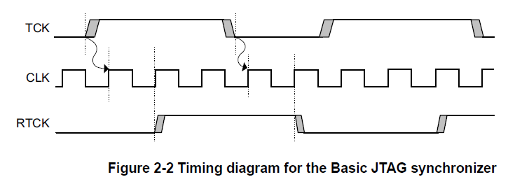
Jtag Timing Diagram
Figure 5 shows a timing diagram for an instruction register access. Some operations occur at the.
 Ddr3 Timing Diagram Wiring Diagram Schematics
Tck test clock input the clock input to the bst circuitry.

Jtag timing diagram. Jtag implements standards for on chip instrumentation in electronic design automation eda as a complementary tool to digital simulation. Before using this manual you should be familiar with the operations that are common to all xilinxs software tools. Arm jtag interface specifications 10 ac timing characteristics 1989 2015 lauterbach gmbh ac timing characteristics important for the timing is that the data on tdi and tms will be sampled with the rising edge of tck will be output on the falling edge and that tdo will change on the falling edge of tck exception see adaptive.
Figure 6 shows timing for a. This document provides you with interesting background information about the technology that underpins xjtag. You do not need to know any of this however to be able to use the xjtag development system as xjtag tests are developed in a high level programming language that does not require any knowledge of the detailed working of jtag.
The characteristics relate to the rvi hardware. Timing requirements for the ieee std. The use of jtag technology arose out of the need to be able to provide sufficient test access for every more complex boards while test access was reducing.
During non jtag operation tms is recommended to be driven high. Figure 3 on page 4 illustrates the timing for transitions to and from jtag flexible mode. Operation of a ieee 11491 jtag boundary scan tap controller.
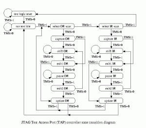
Jtag named after the joint test action group which codified it is an industry standard for verifying designs and testing printed circuit boards after manufacture. Shows how the tap controller operates within a jtag network. Step by step analysis of the tap state machine and timing diagram.
How to bring up the system select a tool for use specify operations and manage design. Jtag port timing characteristics you must consider the timing characteristics of a rvi unit if you design a target device or board and want to be able to connect rvi at a particular tck frequency. Jtag programmer guide i about this manual this manual describes xilinxs jtag programmer software a tool used for in system progamming.
Although tck and tdi can be used as any type of user io in flexible mode it is recommended that these pins are used as outputs. Test logic reset runtestidle. Numbers next to the arrows in the diagram refer to the logic state of tms at the time tck is brought high.
Jtag boundary scan is now a well established technology which is widely used in many areas of test within the electronics industry. Gramming through the jtag interface can be divided into three categories. You must consider them in parallel with the.
 A Jtag Tap State Machine B Simplified Proasic3 Security
 Arm Jtag 信号 Rtck 应该如何处理 Improgrammer 博客园
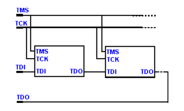
 Jtag Chain Of The Hptdcs Download Scientific Diagram
 Overview Reference Digilentinc
 Virtual Jtag Altera Virtual Jtag Ip Core User Guide
 Arm9tdmi Technical Reference Manual Arm9tdmi Timing

 Jtag Ecc Controller Integration Block Diagram 28
 Pipelined Burst Operation Timing Diagram Burst Write
 Figure 1 From Secure Jtag Implementation Using Schnorr
Training Jtag Interface
 Hd Wallpapers Jtag Timing Diagram Www Love917 Ga
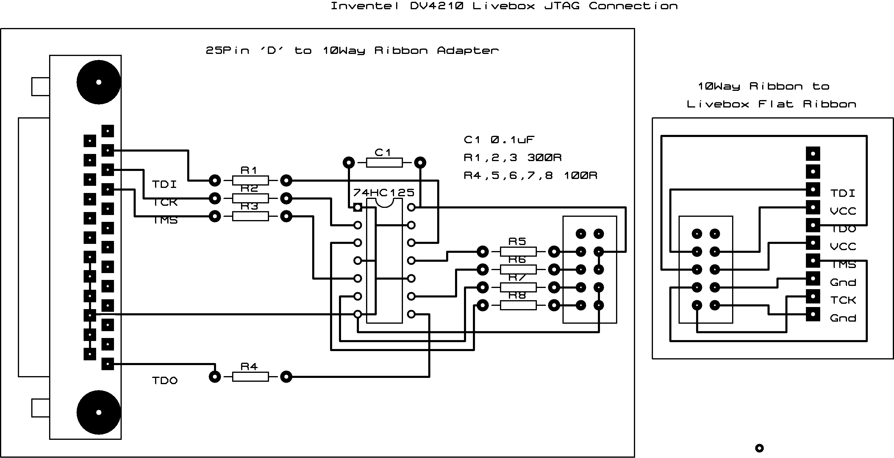
 Connecting Atmel Ice To A Jtag Target Developer Help
 Arm Dstream Pt System And Interface Design Reference Guide
Need Jtag
 Serial Peripheral Interface Wikipedia
 Jtag A Technical Overview And Timing Improgrammer 博客园
 Overview Of The Usb Jtag Hardware Download Scientific Diagram
 Jtag Interface Test Access Port Tap Electronics Notes
 Jtag Hs2 Reference Manual Reference Digilentinc
Training Jtag Interface

 Ieee 1149 Boundary Scan Test Semiconductor Engineering
 Arm Jtag 信号 Rtck 应该如何处理 Improgrammer 博客园
0 Response to "Jtag Timing Diagram"
Post a Comment