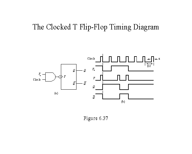
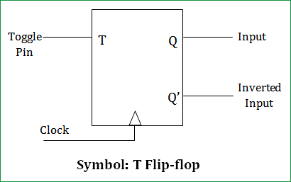
T Flip Flop Timing Diagram
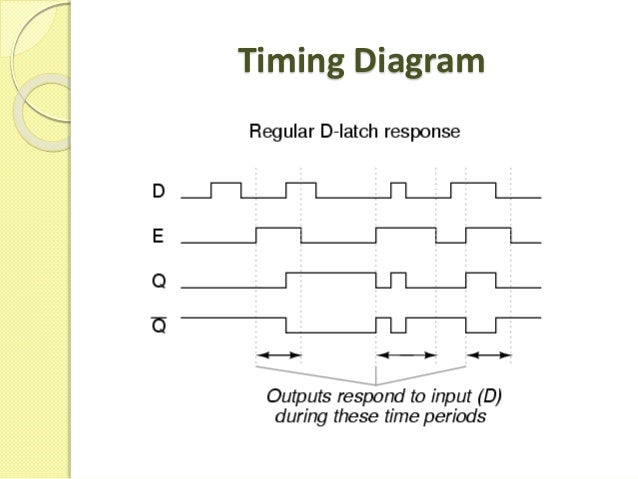
It is the basic storage element in sequential logicflip flops and latches are fundamental building blocks of digital. A timing diagram illustrating the action of a positive edge triggered device is shown in fig.
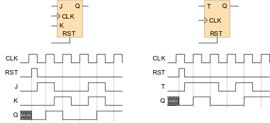
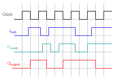
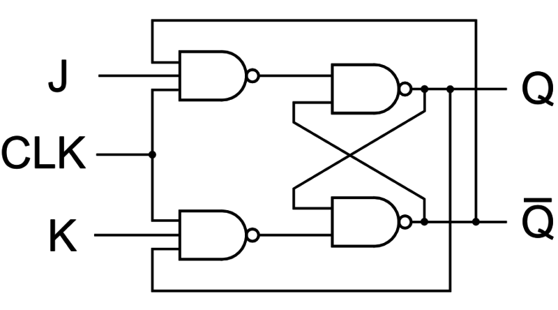
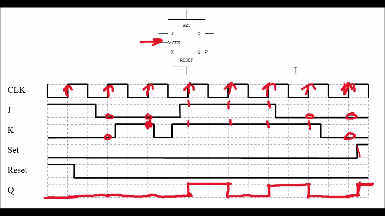 Jk Flip Flop Timing Diagrams
Q goes high and q goes low.
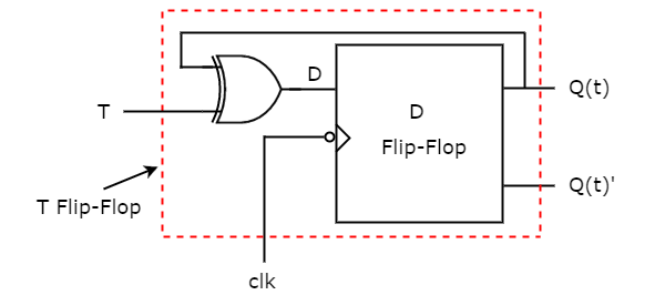
T flip flop timing diagram. Similarly a t flip flop can be constructed by modifying d flip flop. T flip flop is termed from the nature of toggling operation. I think part of the solution provided is incorrect but im not positive so i thought i would ask.
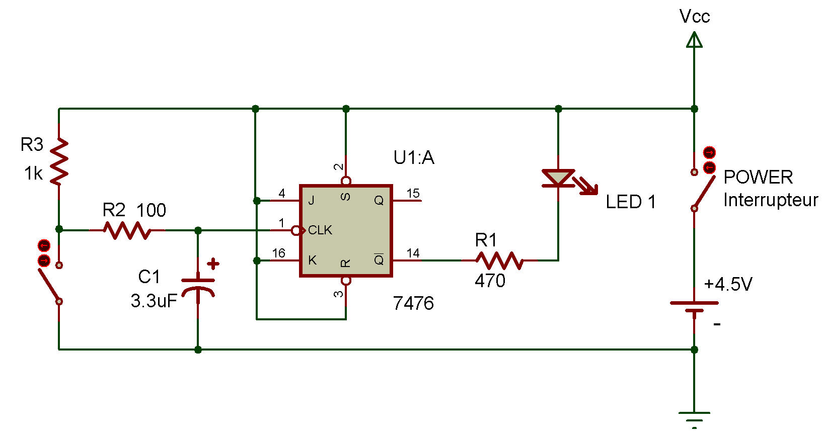
The circuit diagram of a t flip flop constructed from sr latch is shown below. In electronics a flip flop or latch is a circuit that has two stable states and can be used to store state information a bistable multivibratorthe circuit can be made to change state by signals applied to one or more control inputs and will have one or two outputs. At t 1 the toggle changes from a low to a high and the device changes state.
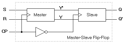
Draw the logic circuit implemented with gates for the sr master slave flip flop in figure 9. Use nor gate flip flops. The major applications of t flip flop are counters and control circuits.
So i was doing some pre midterm studying and i was slightly confused with the operation of this circuit. Overview last lecture introduction to sequential logic and systems the basic concepts a simple example today latches flip flops edge triggered d master slave timing diagrams t flip flops and sr latches cse370 lecture 14 2 the d latch output depends on clock clock high. Enter the expected timing diagram for the signals y y q and q in figure 15.
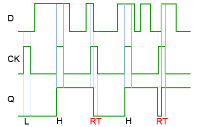
Nand gate flip flop timing diagram master slave flip flop. Here is my attempt so far at filling in the waveforms. Sr master slave flip flop timing diagram edge triggered flip flop.
Toggle t flip flop. In d flip flop the output qprev is xored with the t input and given at the d input. We will assume an initial condition t 0 of q being low and q being high.
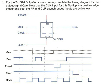
The circuit of a t flip flop constructed from a d flip flop is shown below. The edge triggered d type flip flop with asynchronous preset and clear capability although developed from the basic sr flip flop becomes a very versatile flip flop with many uses. Input passes to output.
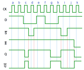
I believe the value of b provided at. T flip flop is modified form of jk flip flop making it to operate in toggling region. The timing diagram in figure 3 15 view b shows the toggle input and the resulting outputs.
 Flip Flops Reference Digilentinc
 Solved 1 Assume The Initial Condition Of Qs Is 0 Comple
 What Is The Problem Of S R Flip Flop How Can D Flip Flop
 T Flip Flop Circuit Diagram Truth Table Working Explained
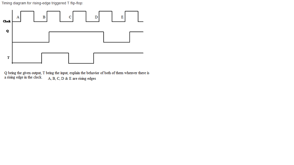 Solved Timing Diagram For Rising Edge Triggered T Flip Fl

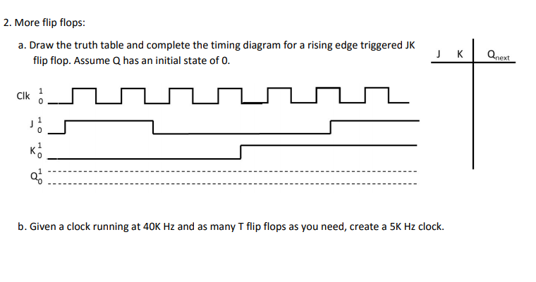 Solved 2 More Flip Flops A Draw The Truth Table And Co
 Counters In Digital Logic Geeksforgeeks
 Flip Flops Registers Counters And A Simple Processor Pdf
 T Flip Flop Circuit Diagram Truth Table Working Explained
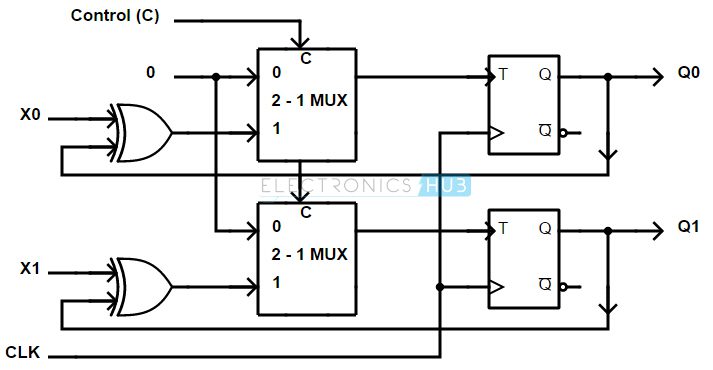 Designing Of T Flip Flop
Digital Circuits Conversion Of Flip Flops Tutorialspoint
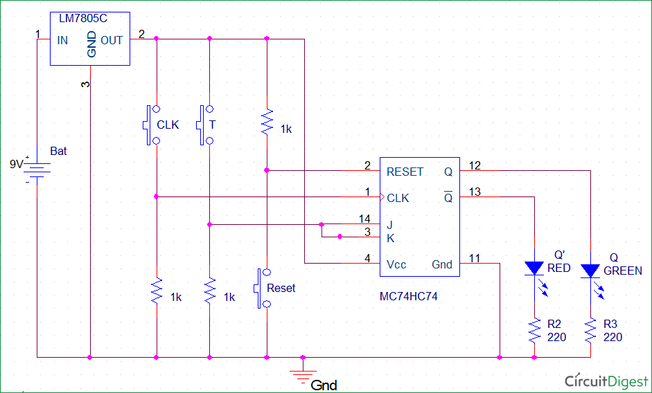
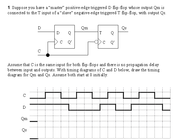 Solved Suppose You Have A Master Positive Edge Triggered
 Flip Flops Digital Circuits 4 Sequential Circuits
 Flip Flop Truth Table Various Types Basics For Beginners

 Jk Flip Flop And The Master Slave Jk Flip Flop Tutorial
 D And T Flip Flop
0 Response to "T Flip Flop Timing Diagram"
Post a Comment