Consider The Circuit Diagram Depicted In The Figure
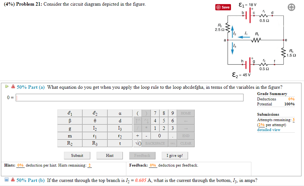
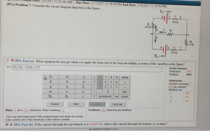
A what equation do you get when you apply the loop rule to the loop abcdefgha in terms of the variables in the figure. Consider the 10 ω resistor having current ib.
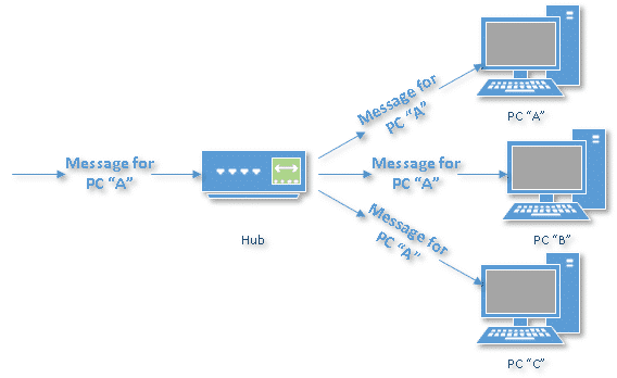 What S The Difference Between A Hub A Switch And A Router
The loop will act as a magnet and there will be force repulsion.

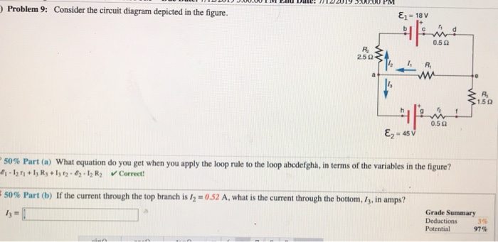
Consider the circuit diagram depicted in the figure. Consequently the value of the current ia in figure 5 is equal to the value of the current ia in figure 6b. Consider the circuit diagram depicted in the figure. A what equation do you get when you apply the loop rule abcdefgha in terms of the variables in the figure.
For the action depicted in the figure figure 1 indicate the direction of the induced current in the loop clockwise counterclockwise or zero when seen from the right of the loop. είconsider the circuit diagram depicted in the figure. The recognizer has a single input x and a single output y in addition to an asynchronous reset signal.
B draw the complete 4 4 rom circuit using your switches from part a. For the above recognizer described above. This time the voltage across each of these elements of the circuit is the same.
It is known that twobattery internal resistors r1and r2 are both 02ω 12v and 24v. The circuit shown in figure 6b is equivalent to the circuit shown in figure 5. B if the current through the top branch is i 2 038 a what is the current through the bottom i 3 in amps.
It is known that two25ω24v and ε236v. On the diagram it is represented by the vector labeled v0. R2 16ω2and rs 262 but ri is unknown.
Consider the circuit diagram depicted in the fgure. On the diagram it is represented by the vector labeled. The recognizer sets the output y to 1 if the input signal x was equal to 1 in at least 3 clock cycles after the reset was disasserted.
Now consider a diagram describing a parallel ac circuit containing a resistor a capacitor and an inductor. Each x in the figure represents a switch that determines whether the rom produces a 1 or 0 when that location is read. A show how a switch x can be realized using a single nmos transistor.
Consider the circuit diagram depicted in the figure. B if the current through the top branch is i2 0605 a what is the current through the bottom i3 in amps. R2and r3 40f but ri is unknown.
Internal resistors r1 and r2 are both 02n. Consider a diagram describing a parallel ac circuit containing a resistor a capacitor and an inductor. This time the voltage across each of these elements of the circuit is the same.
With four rows and four columns is depicted in figure p63. Figure 6c shows the circuit from figure 5 after labeling the value of the current ia.
 Logic Circuits An Overview Sciencedirect Topics
 Implementation Of A Toffoli Gate With Superconducting
 Consider The Following Circuit Diagram If R1 R2 R3 R4 R5 3
A Futuristic View Of Building Distributed Systems With Messaging
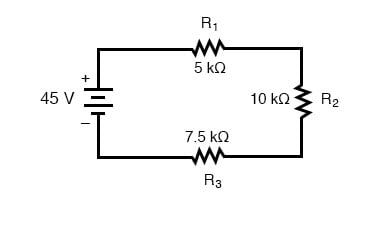 Voltage Divider Circuits Divider Circuits And Kirchhoff S
 Solved Consider The Circuit Diagram Depicted In The Figur
Deconstructing Lottery Tickets Zeros Signs And The
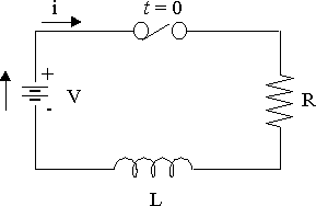 5 Application Of Odes Series Rl Circuit
 Efficiently Design An Op Amp Summer Circuit Electronic Design

 Emulator Circuits And Resistive Switching Parameters Of
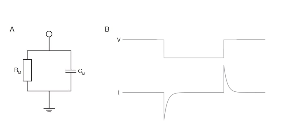 Understanding The Cell As An Electrical Circuit
 Temporo Insular Enhancement Of Eeg Low And High Frequencies
Examples Of Solved Problems For Chapter 3 5 6 7 And 8
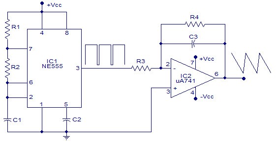 Square Wave Generator Using Op Amp Electronic Circuits
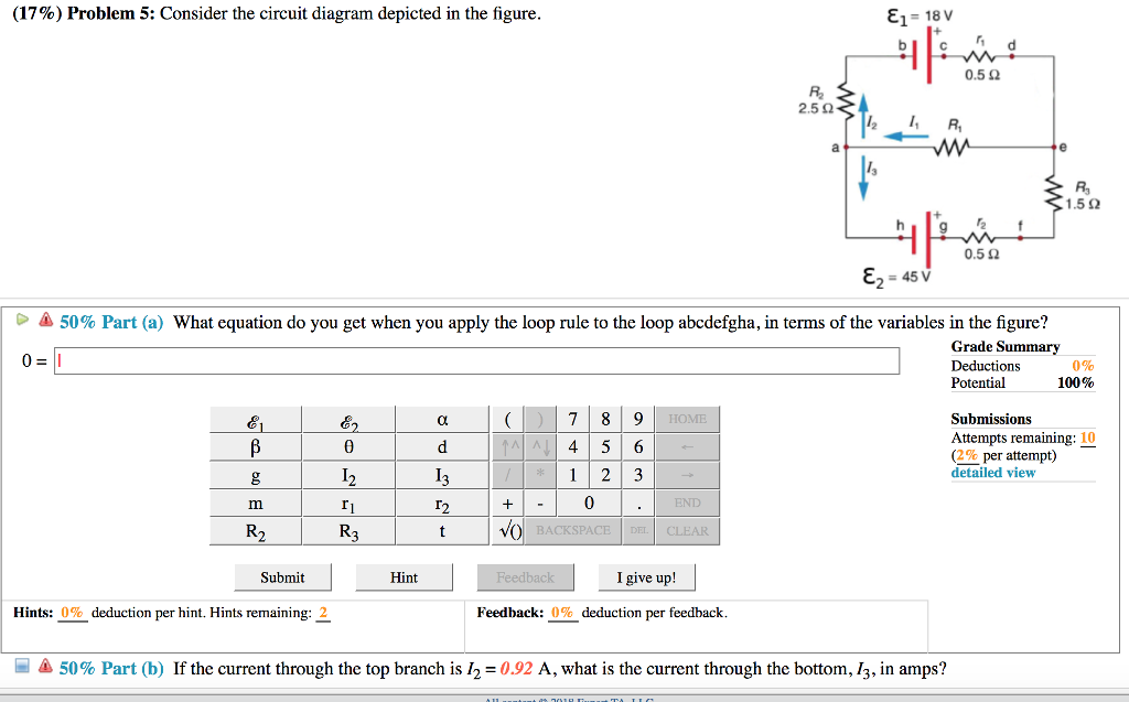 Solved 17 Problem 5 Consider The Circuit Diagram Depi
 Solved Problem 9 Consider The Circuit Diagram Depicted I
Computer Setup
Open Source Software In Quantum Computing
 Square Wave Generator Using Op Amp Electronic Circuits
 Consider The Circuit Diagram Depicted In The Figure Free
 Circuit Diagram Wikipedia
 Wien Bridge Oscillator Tutorial And Theory
 A Framework For The Modular And Combinatorial Assembly Of
Computer Setup
 Ac Dc Converters Including Buck Boost And Flyback
0 Response to "Consider The Circuit Diagram Depicted In The Figure"
Post a Comment