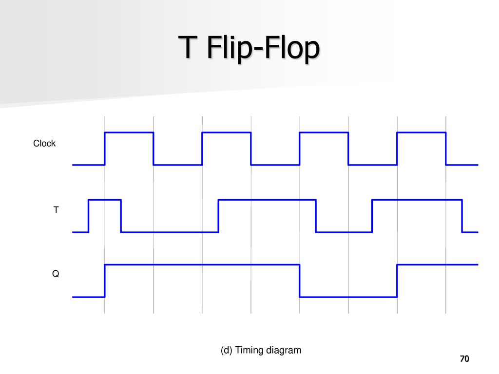
Toggle Flip Flop Timing Diagram
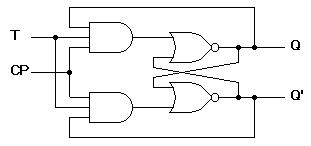
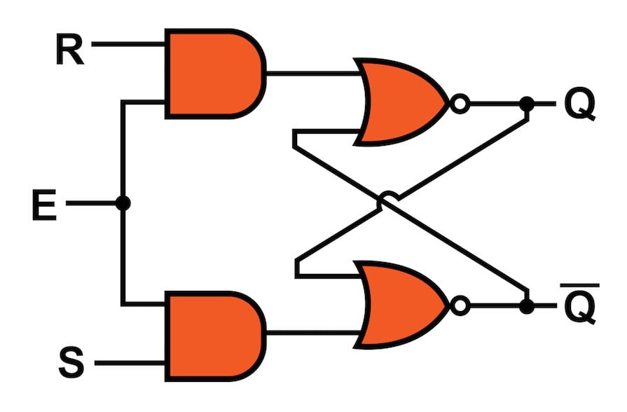
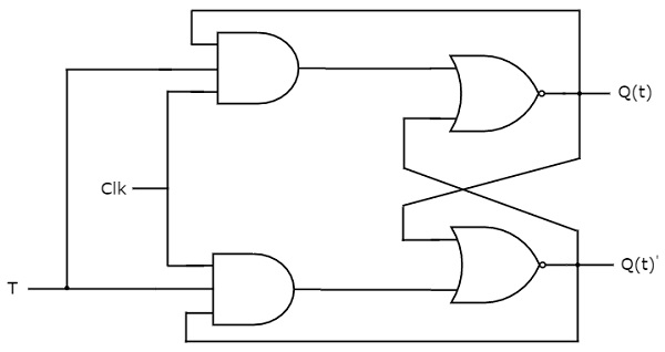
In d flip flop the output qprev is xored with the t input and given at the d input. The circuit diagram of a t flip flop constructed from sr latch is shown below.
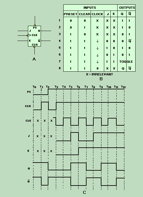
The actual input is now ck.

Toggle flip flop timing diagram. Due to its versatility they are available as ic packages. Jk flip flop timing diagram the jk flip flop augments the behavior of the sr flip flop jset kreset by interpreting the j k 1 condition as a flip or toggle command. This flip flop has only one input along with clock pulse.
The major applications of d flip flop are to introduce delay in timing circuit as a buffer sampling data at specific intervals. Suppose that initially ck and q 0. T flip flops are handy when you need to reduce the frequency of a clock signal.
Then q and d must be 1. Q goes high and q goes low. These flip flops are called t flip flops because of their ability to complement its state ie toggle.
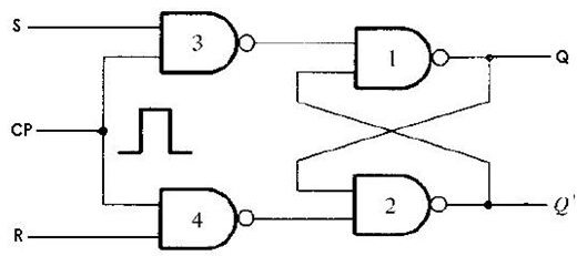
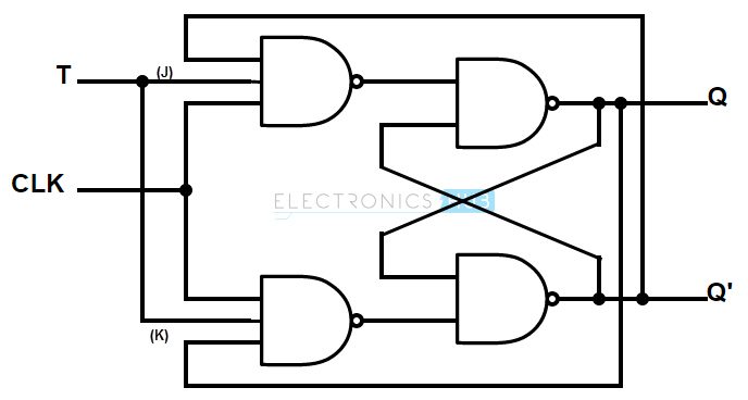
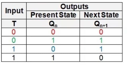
D flip flop can be built using nand gate or with nor gate. When t1 and cp1 the flip flop complements its output regardless of the present state of the flip flop. Jk flip flop jack kilby t flip flop toggle out of the above types only jk and d flip flops are available in the integrated ic form and also used widely in most of the applications.
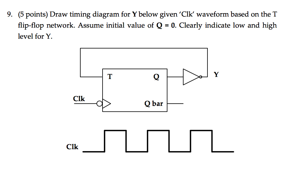
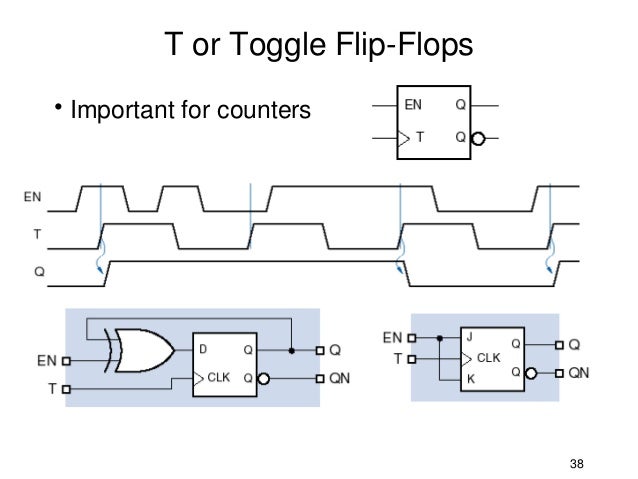
If you keep the t input at logic high and use the original clock signal as the flip flop clock the output will change state once per clock period assuming that the flip flop is not sensitive to both clock edges. D flip flop is simpler in terms of wiring connection compared to jk flip flop. Input passes to output.
So these flip flops are also called toggle flip flops. 538 using a positive edge triggered d type flip flop. At t 1 the toggle changes from a low to a high and the device changes state.
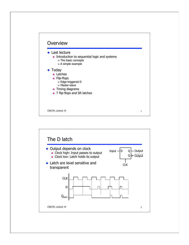
The name t flip flop is termed from the nature of toggling operation. Here in this article we will discuss about t flip flop. Overview last lecture introduction to sequential logic and systems the basic concepts a simple example today latches flip flops edge triggered d master slave timing diagrams t flip flops and sr latches cse370 lecture 14 2 the d latch output depends on clock clock high.
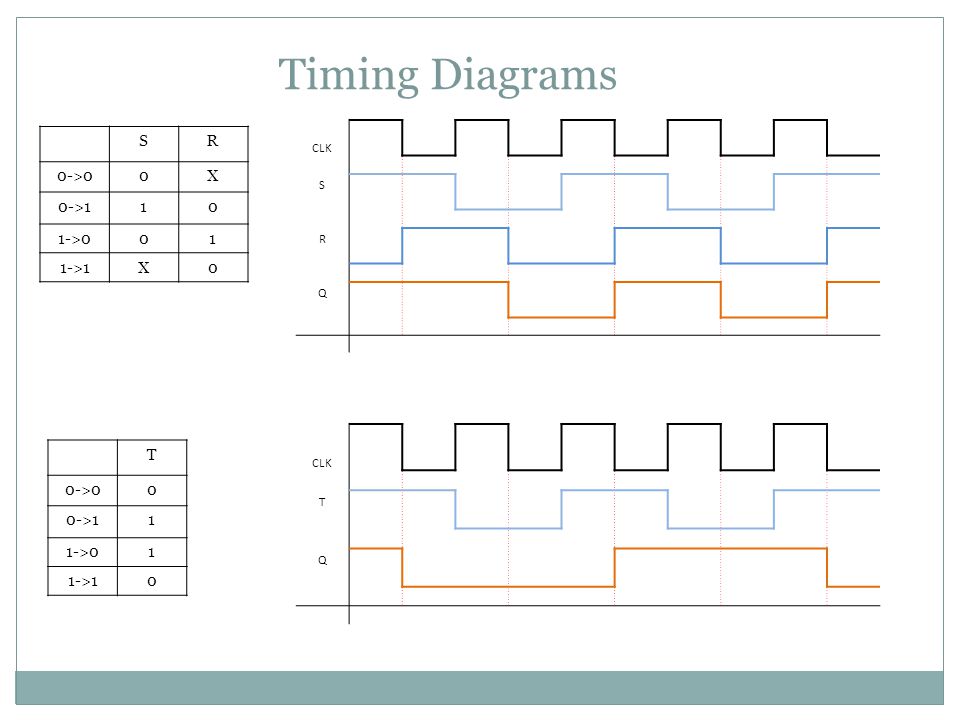
Toggle t flip flop. So they are called as toggle flip flop. We will assume an initial condition t 0 of q being low and q being high.
Similarly a t flip flop can be constructed by modifying d flip flop. The effect of this mode of operation is also shown in the timing diagram in fig. The timing diagram in figure 3 15 view b shows the toggle input and the resulting outputs.
 Solved Draw Timing Diagram For Y Below Given Clk Wavefo
 Types Of Flip Flop Circuits Explained Rs Jk D T
 Counters In Digital Logic Geeksforgeeks
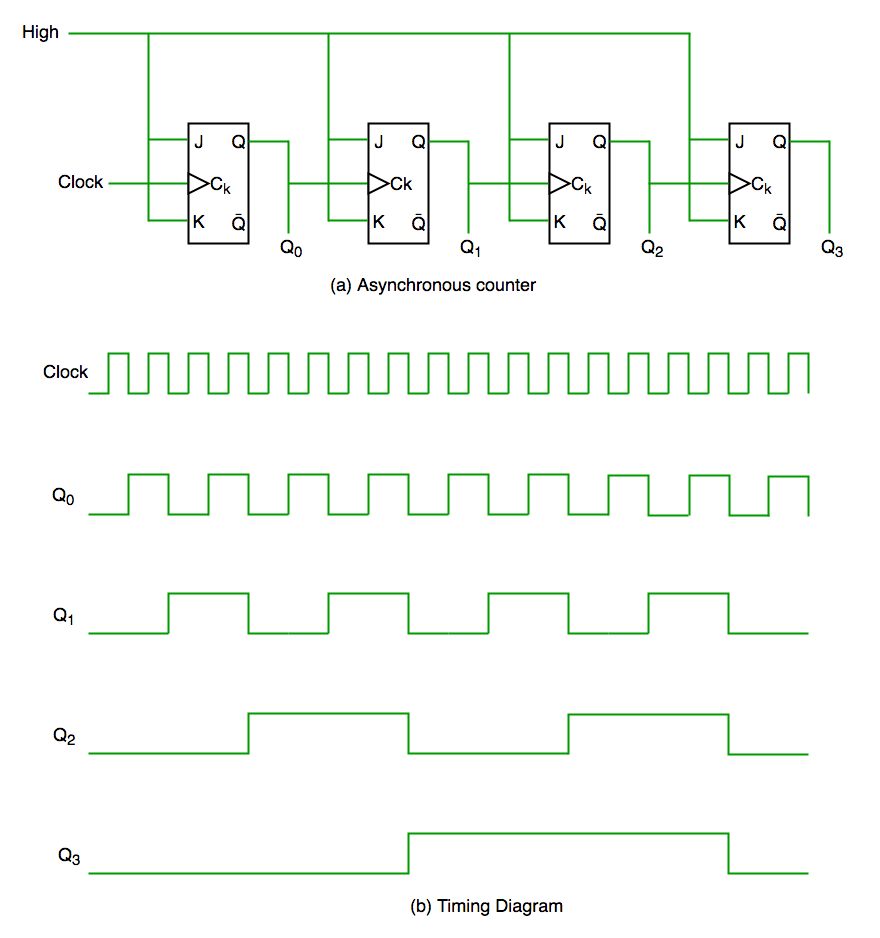
 Asynchronous Counter T Flip Flop Timing Diagram Wiring
 Flip Flops
 Ekt 121 4 Digital Electronics I Ppt Download
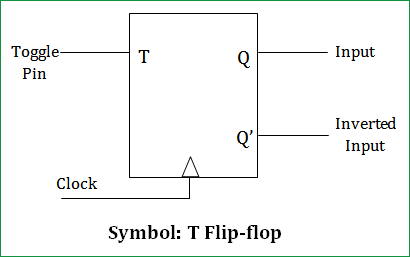
Designing Of T Flip Flop
 T Is For Toggle Understanding The T Flip Flop
Timing Diagrams For D Flip Flops Physics Forums
 Designing Of T Flip Flop
 Learn Digilentinc Flip Flops
 Sequential Logic Circuits Flip Flop Pt 3
 Designing Of T Flip Flop
 Chantha Thoeun Flip Flop Circuits Types Of Flip Flops Sr

 Frequency Division Using Divide By 2 Toggle Flip Flops
 D And T Flip Flop
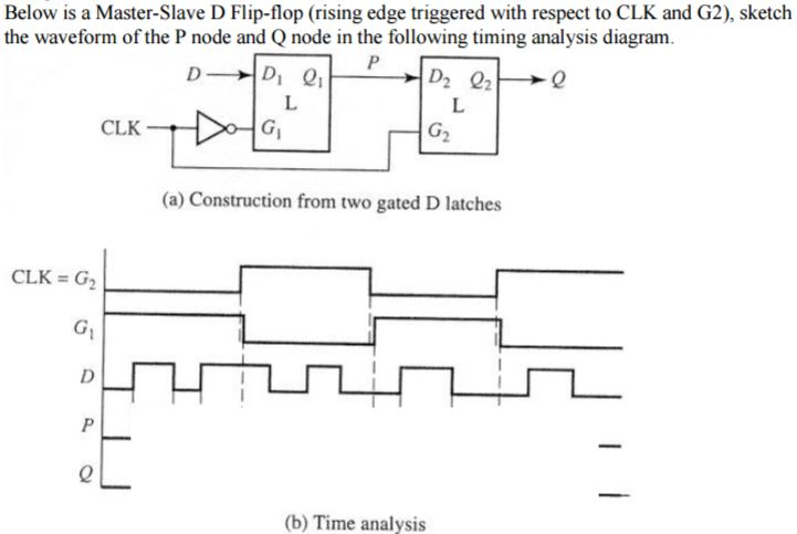 Positive Edge Triggered Master Slave D Flip Flop Timing
![]() Flip Flop Electronics Wikipedia
Flip Flop Electronics Wikipedia
 T Flip Flop Circuit Diagram Truth Table Working Explained
 T Flip Flop Circuit Diagram Truth Table Working Explained
 Sequential Circuits Flip Flops Part 2
 Digital Circuits Flip Flops Tutorialspoint
 T Is For Toggle Understanding The T Flip Flop

0 Response to "Toggle Flip Flop Timing Diagram"
Post a Comment